

- ? Instrument
- ? Instrument
- ? Instrument for Silicon Material
- ? Instrument for CZ&DSS
- ? Instrument for Wafer
- ? Instrument for Solar Cell
- ? Instrument for Module
- ? Instrument for PV Station
- ? LED instrument
- ? Other instrument
- ? Consumables
- ? Consumables
- ? Accessories
- ? Software
- ? Process software
- ? System software
- ? Application Software
- ? Intrument exchange
- ? Overview
- ? Exchange flow
- ? Exchange notice
- ? Exchange Center
- ? Maintenance Service
- ? PV Equipment Upgrades
- ? Auxiliary Equipment Maintenance
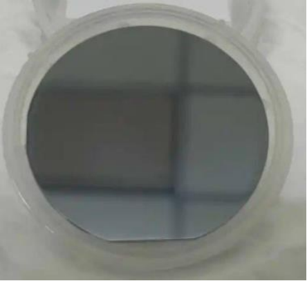
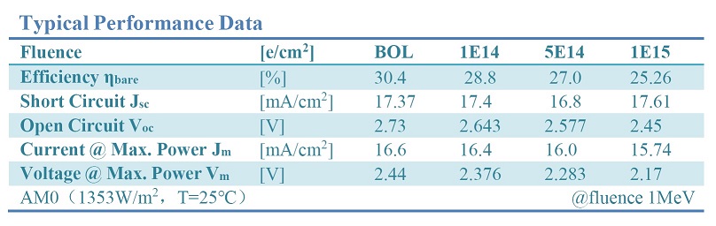
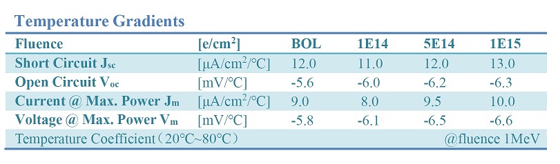
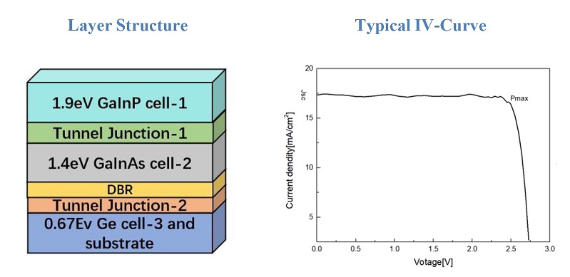
Consumables >> Consumables >> GaInP/GaAs/Ge Epitaxial Wafer-30% Triple Junction
                The  unprocessed Epitaxial Wafers of class 30% contain our high-efficiency GaInP/GaAs/Ge based epitaxial layers on a Ge substrate. These epixial wafers can be used for any further processing and customized cell designs.


Design and Mechanical Data
  Substrate Material :GaInP/GaInAs/Ge on Ge substrate Base Material :100 mm ±0.20
 Thickness :145 μm ±15 μm or 175 μm ±15 μm
 Major Flat length :32.5 mm ±2 mm
 Major Flat orientation:(100) ±2°

 Average Weight :≤ 93 mg/cm2
 Laser mark label:Alpha-numeric
?2008-2050 HenergySolar. All rights reserved