

- ? Instrument
- ? Instrument
- ? Instrument for Silicon Material
- ? Instrument for CZ&DSS
- ? Instrument for Wafer
- ? Instrument for Solar Cell
- ? Instrument for Module
- ? Instrument for PV Station
- ? LED instrument
- ? Other instrument
- ? Consumables
- ? Consumables
- ? Accessories
- ? Software
- ? Process software
- ? System software
- ? Application Software
- ? Intrument exchange
- ? Overview
- ? Exchange flow
- ? Exchange notice
- ? Exchange Center
- ? Maintenance Service
- ? PV Equipment Upgrades
- ? Auxiliary Equipment Maintenance
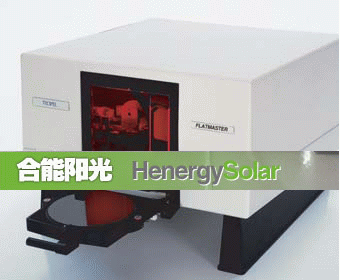
Product Brief:
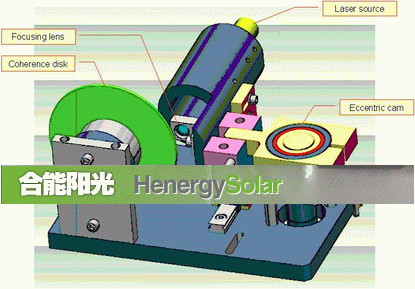
Sapphire/SIC wafer flatness and surface appearance system provide a previous surface flatness testing solution, though non-contract lighting testing to record the whole information of the surface, rapid and fast measurement for various of surfaces, line and all kinds of surface information.
Product Feature:
■ Non contract and non damage testing.
■ For all kinds of material: semiconductor, metal, glasses…..
■ For all kinds of wafers: Sapphire, Sic, GaAs,SiO2,Ge, LiNbO3
■ For all kinds of surfaces: Abrasive surface, Polished, Ultra-smooth surface
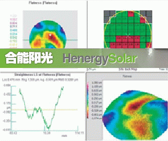
■ can test several informations:Thickness,TTV,SORI,LTV,LDOF,Pressure,BOW,Curve,Flatness,
planeness,line Contours,surface contours
■ Wholly analyze system,for all kinds of surface.
■ Automatic,Rapid,accuracy and stable.
■ Over 15 years for industry and over hundreds application.
Technical Information:
■ Accuracy: 50nm (2.0μ″)
■ Repeatable: 15 nm(0.6μ″)(1 sigma)
■ Resolution: 5nm (0.2μ″)
■ Sample size: 25mm-200mm
■ Number of testing points: 230,000 / measurement
■ Testing time: 5s
■ Power supply: ~220V 50Hz
Customer:
Honeywell Electronic Materials,SEI,Showa Denko,SESMI,Saint Gobain,Nikko Materials,Hitachi Cable,Freiberger Compound Materials,Crystal Tech,Samsung,LG,Crystalwise,Wafer Works……